Charge Domain Digital
Charge Domain Digital Processing
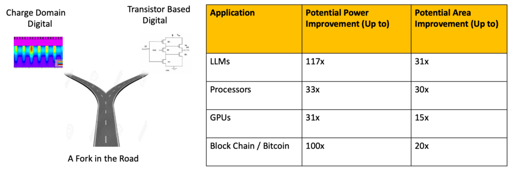
Charge Domain Digital Processing. Digital processing has long been associated with transistors. The truth is that transistors are not an ideal technology for digital processing. This is because they crowd the current into a small channel like a Fin which slows electron transfer and maximizes trap, thermal and defect related noise. Its also very leaky due to the small distance between critical implants and extremely inefficient to metalize. A much better technology is AIStorm’s charge domain processing (patented and patent pending). Charge domain process can improve performance significantly versus transistors, reduce power consumption by up to 117x, and reduce footprint by up to 30x. The best part is that charge domain processing is compatible with deep submicron processes such as 5nm or smaller lithographies, and often does not require process changes to implement. Additionally, we work with customers on those parts of their circuits most requiring improvement leaving the rest built from transistors. Charge domain processing allows lithographies to act several nodes smaller in terms of performance dramatically reducing costs.
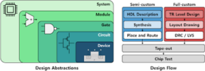
Ease of Adoption – Compatible with Existing Digital EDA Flows. AIStorm’s Charge Domain digital structures are compatible with standard digital flows. Transistors eventually become polygons at the most basic level, just as do charge domain structures. Our digital primitives can be defined using the same high level Verilog or HDL through synthesis and place & route, with the same types of verification and timing files that transistor based primitives offer. We can even co-exist in the same PDK or have gate alternatives or switches within specific macroblocks as transistor based primitives.
Sounds too Good to be True. It does but it is true. We have worked with some of the world’s largest companies to implement improvements to their existing designs using charge domain technology. The fact is that foundries have grown so accustomed to transistor only based designs that they have stopped considering other methods. If you have a design that needs an improvement we can quickly work with you to produce a proof of concept.
GPUs and Processors. GPUs and Processors can see a performance >10x performance improvement, 15x size reduction and 31x power reduction. With the estimates for server power forecasting an additional terawatt of power in just the next few years charge domain can be a life saver. Charge domain is especially capable of matrix & shift register moves which are common in GPUs.
Large Language Models (LLMs). The general purpose transformer (GPT) is extremely well served domain structures. In fact power reductions can be as much as 117x lower for an existing designed re-synthesized in the charge domain.
Bitcoin and Block Chain. Block chain and the mining process (SHA and encryption) are processes that are highly dependent on shift register manipulation and basic mathematical operators. Charge domain shift registers do not flush charge, do not have the shoot through currents and do not have the leakages the way that shift registers do in the digital domain and that is part of the reason they can be improved so significantly by charge domain. Transistors just cannot move charge as quickly based on basic physics.
Training Appliances. AI training is one of the most computationally intensive operations. Use of charge domain digital can improve silicon area performance by up to 300x in a deep submicron node.
years
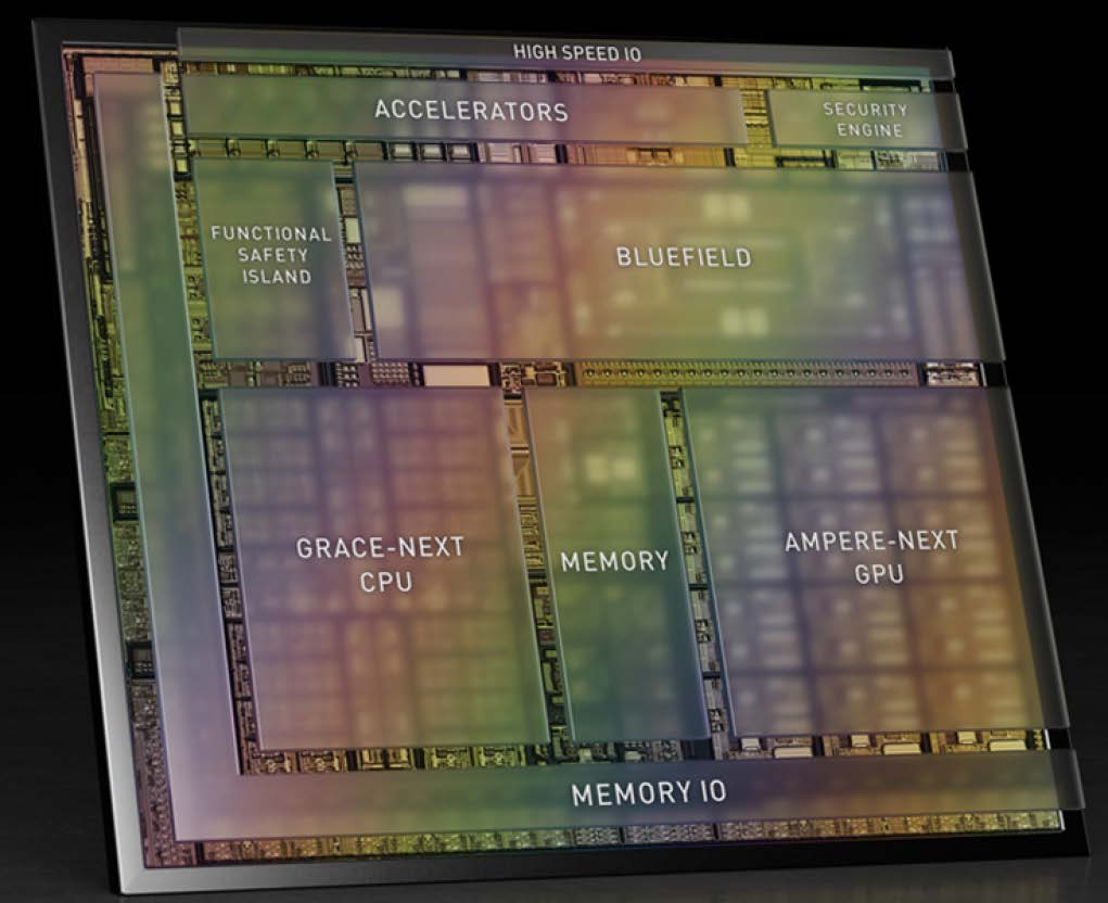
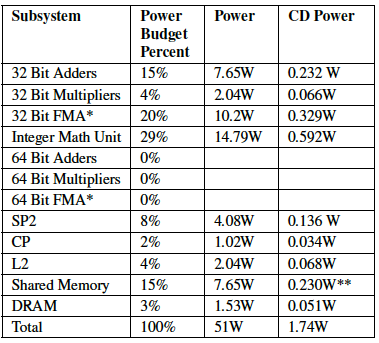
Power Improvements. Deep submicron designs such as 2nm->14nm use special configurations including FinFETs, GAA (gate all around), nanowires and other structures. All these structures involve a channel that is turned on or off to allow current flow. These devices are so small that they have effects which cause Vt variation between on and off conditions, and excessive leakage. The table to the left shows the power savings of charge domain replacing certain structures in a GPU such which are an integral part of the GPU structure illustrated above. Best of all it is only necessary to replace specific circuits since charge domain can coexist with your digital designs and can be made part of the same EDA digital flow. Often there are no process changes required. In the Figure the Power is the power using transistors and to the right labelled CD power is the charge domain power for the same circuit. In addition to power savings significant area and performance enhancements also can be expected.
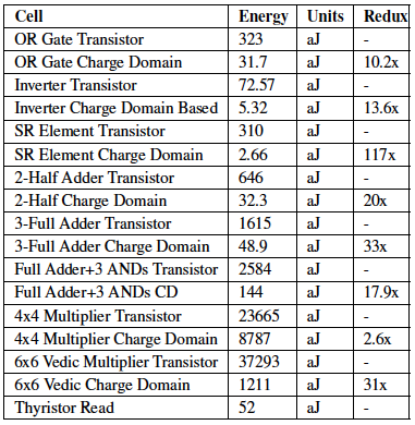
Digital Block Improvement. The table to the right illustrates some power improvements (energy per cycle) for some basic cells comparing the original transistor based implementation to a charge domain implementation. The unit for energy is aJ or attojoules or 1e-18J. In addition to the power improvements shown performance improvements of >10x and size reductions of up to 30x can also be expected many cases.
The good news is that AIStorm can work with your existing EDA flow and implement a proof of concept often without any processes changes on a development run even in the PCMs or scribes. If you have a performance, power or size issue let us help you overcome it.
For those working with pixels AIStorm can accept charge directly from pixels and has TCAD engineers with decades of pixel experience who can help optimize designs from low light through high speed.
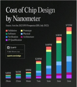
Cost Improvement. The figure to the left shows the estimated costs of deep submicron developments according to ARM Inc. A significant portion of this is the cost validation, software, verification tools, IP Qualification and prototypes. AIStorm’s Charge Domain Domain digital can offer a performance improvement of one to two generations of lithography and in some cases even more. Imagine turning a $725M project into a $449M project while maintaining performance, area and improving power and leakage.
Call AIStorm today for more information or to schedule a meeting!