Charge Domain Memory
Charge Domain Memory - SRAM & DRAM
SRAM (Layout Image Courtesy of Microwind)
SRAM or static ram means that the information it stores stays resident indefinelty while power is supplied. SRAM does not scale in deep submicron processes. For example at 5nm the SRAM is 0.0201um^2 and smaller lithographies the cell size is basically the same. In fact from about 12nm the SRAM is contact limited (see Figure 2). A charge domain SRAM cell memory element overcomes this limitation in an area smaller than a single FinFET in a given lithography. This means that the charge domain element is about 1/10th of the size of the standard transistor based cell and even smaller compared to isolated or ULP (ultra low power) or isolated cells. The memory element uses charge domain techniques in a way that has never been done before. The memory element is reliable with robust immunity against false actuations and errors from disturbances. The leakage current of the SRAM is about 1pA at 5nm compared to 42pA for a conventional SRAM. Isolated or ULP cells leak less but at an area cost. Charge domain also supports lower leakage variants.
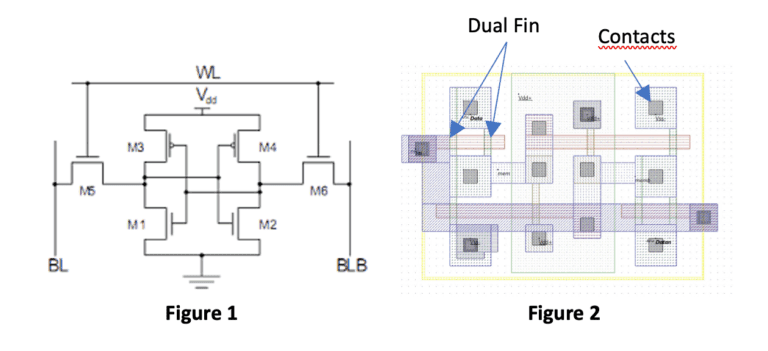
The Fin Lithography Doesn’t Matter below 12nm. The fundamental schematic cell of SRAM using transistors is shown in Figure 1 above. M1 to M4 are the inverters parallel to each other. M5 and M6 are the word lines and BL and BLB the bit lines. The layout (a top view of the polygons that are used to make the actual devices on silicon) is shown in Figure 2. In this example we are looking down the transistors created by the red poly where the active (green) crosses it. The Fins are the thin green lines crossing the red poly. For example we have labelled a dual Fin FinFET with “Dual Fin.” There are several other single and dual Fin FinFETs in Figure 2. Notice all the empty space around and between the Fins and the big drain and source regions with contacts surrounded by active on either side. Also notice the box in the middle. This is an n-implant used to create the p-channel devices and also has spacing requirements. The interesting thing about the SRAM cell, which is one of the fundamental cost adders for modern electronics, is just how much space is wasted in the cell itself.
10x Smaller. The SRAM cell in Figure 2 is contact limited. The contacts are the small squares, one of which is labelled “Contacts” in the the middle of highly doped active regions. This is where the metal (connection wires) actually attach to the FinFETs, to the gates and to the outside world. There is a physical limit to the size of the metal which is needed to create a contact. Further, the contact must be surrounded by a certain amount of highly doped silicon to create the drain and source regions. This puts the limit on the FinFET size and ultimately to the size of the overall SRAM. Note that even if we were to make the 5nm fin of
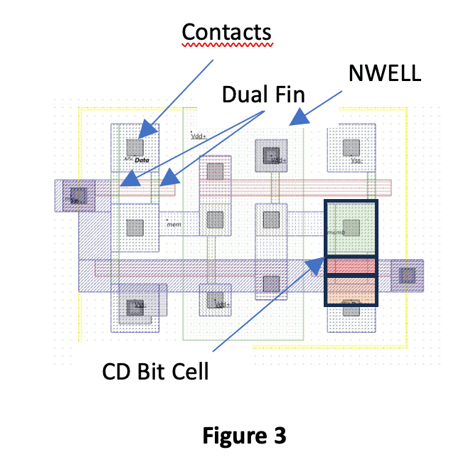
the FinFET smaller it would really make no difference. 2nm, 3nm, 5nm, it would pretty well look the same since it is not the fins that are setting the size of the cell. This is not intuitive since we have been trained that the size of silicon features shrinks with lithography but really that is not the case here. Additionally, the nwell implant is not required for charge domain implementation which allows elements to be packed close together.
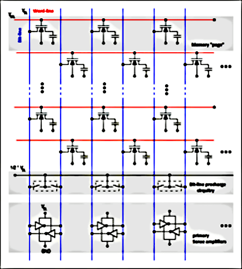
Charge Domain is Not Contact Limited. A fundamental difference between voltage domain devices like FinFETs and the charge domain devices that AIStorm uses is that charge domain devices do not require contacts throughout the body of the circuit, only when returning information to the voltage domain so that it can be compatible with voltage domain circuitry on the same chip. This means that most of the contacts can be removed. The charge domain equivalent of a MOSFET switch also does not require the highly doped drain and source regions, which makes them much smaller than the FinFETs in the Figures above (imagine the contact and region around the contact removed and only the fin regions left). AIStorm has pioneered a unique technology called the CD superjunction which allows digital gates to accept charge input from the previous gate and automatically process the result to a charge output without requiring a clock. It can be seen from Figure 3 that if we remove most of the contacts and replace them with the small rectangle with the three colors (equivalent AIStorm circuit area) in the lower right hand corner then we are 10x smaller. It is very expensive to create SRAM in small lithography processes because we are paying for 12nm real estate at 2nm prices. Not with AIStorm’s charge domain digital memory.
14x Lower Power. The back to back SRAM cell has a shoot through current as the lower switch turns on and the upper switch turns off, during its operation and vice versa. Additionally, all the of highly doped drain and source contacts have an overlap capacitance with the gate that stores energy with each transition and is flushed with the next transition. Charge domain does not flush and refill, rather it just moves charge and saves all this waste. Additionally, the close proximity of the highly doped regions and the damage done by the smashing of the metal into the crystal lattice produces leakage current that adds up significantly over a large memory array. Charge domain does not have these highly doped regions in close proximity, nor does it smash metal into the lattice as many times, reducing defects which cause leakage. These factors combine to reduce power significantly when using charge domain SRAM vs. standard transistor based SRAM.
>2.5x Faster. It can be shown the charge domain memory will always be 2.5x or more faster than transistor based memory. This can be most easily understood by considering again Figures 2 and 3 where the capacitances and the lengths of travel of electrons collude to require more electrons and also to take longer to traverse their path through the circuit. The collective RC time constant, and mean free path, as electrical engineers would call it, is much longer for a transistor based circuit than a charge domain circuit. Therefore not only do we get smaller and lower power, but we also get faster. Normally, the speed increase is more than 2.5x since this 2.5x is the ideal case for the most optimized process and most processes are not the most idealized case.
More Reliable. Reliability is a critical factor in memory where large arrays are repeated massively. As described previously each of the contacts in the Figures 2 & 3 have the potential to cause defects. Additionally the interaction between the highly doped regions around the contacts with the fins themselves also have a probability of producing defects. Charge domain has a tiny fraction of the number of these contacts, is much smaller due to the removal of all those drain and source highly doped regions, and where it has highly doped regions they are not as close to each other. Defect density, the common measure of defects per unit area, also benefits charge domain since the bitcell is just smaller. For this reason charge domain is always more reliable than a transistor based solution for a given amount of memory in a given process.
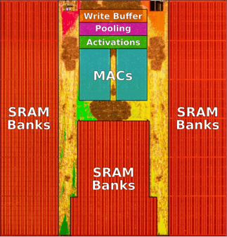
DRAM. DRAM or dynamic ram is very different to SRAM. Dynamic RAM only holds its value for a short time (10’s of milliseconds) and must be regularly refreshed or it will lose its information. DRAM is made using a capacitor and a switch. The switch is a MOSFET like a FinFET. Figure 4 illustrates an array of DRAM on top and SRAM on the bottom with both connected to reader lines. Processes optimized for high speed, like those used to make GPUs or CPUs, try to minimize size and maximize drive strength. This makes them leaky. It means that DRAM needs a bigger capacitor and SRAM also leaks more than they would in an ideal memory process. For small lithography processes the highly doped
drain and source regions makes it very difficult to keep the switches from leaking between these two regions. Therefore normally the smallest switches cannot be used. For all of these reasons it has become the default standard to separate memory from processors and not to put them on the same silicon. Of course this means that different pieces of silicon talking and this is what all the new coupling methods (CoWoS, UCIe, EOE, etc. are all about).
Charge Domain Allows Mixing of High Speed Logic and Memory. The dynamic market for memory ushered in by the AI wave has produced many advancements in memory including high bandwidth (HBM) memory and distributed memories optimized for AI processing. Regardless, the limitations described earlier remain. AIStorm does not use transistor based switches, does not put drain and source highly doped regions in close proximity of one another, and does not have large numbers of overlap capacitances extending the time constant of the circuits. AIStorm’s charge domain DRAM also does not use capacitors in series with switches. For all of these reasons the limitations that separated memory from compute in the past need not be maintained with AIStorm’s charge domain. As a lot of effort is going into optimizing the interconnects between the compute and the memory chips to save power and increase speed, these efforts can also be overcome using charge domain and are not necessary.
Memory in AI
Memory is the biggest cost in AI and its biggest user of power. In Figure 6 this is illustrated by coloring the memory, in this case SRAM, in the top down view of a Tesla GPU. The SRAM is red, the metal interconnects (wires) to the memory are gold. The actual AI part is the small blue area labelled MACs, green area labelled activations, purple area labelled pooling and orange area labelled write buffer. Figure 6 illustrates one of the biggest disadvantages of transistor based digital processing. It can be seen that although this chip is said to be an AI chip, in reality it is a memory chip with some AI on board (MACs, Activitations, Pooling, Write Buffer).
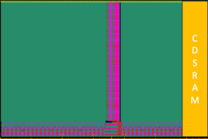
Size Reduction Comparison
Figure 7 shows an SRAM array consisting of two large pages of equal size (not completely shown). The CDSRAM area in yellow completely replaces the two banks of SRAM with the same amount of memory. This illustrates the significant improvement possible using AIStorm’s charge domain SRAM.