Charge Domain Dataconverters
Charge Domain Dataconverters
Dataconverter Fundamental Analog Limitations
Dataconverters such as sigma delta data converters allow the conversion of analog values to digital values or vice versa with significant accuracy. For example 24 bit analog to digital systems are available commercially with a common ENOB (equivalent number of bits) of 18 bits or so. This is a remarkable level of accuracy considering all of the sources of errors, including noise, that lurk within an analog circuit. With an accuracy of 18 bits we are saying that we can be sure we are within +/-0.0001907% of the actual value we are converting. Sigma delta dataconverters do this by using a method called digital feedback. There are different kinds of dataconverters, some of which are focused on speed, and some on area efficiency or power efficiency, however, we will focus for now on sigma delta dataconverters which are focused on precision.
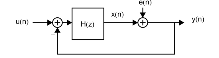
Sigma Delta Converters are Simple Sampling Math Constructs. Sigma delta dataconverters are purely mathematical constructs that are turned into circuitry. We will discuss that circuitry in a moment, however, the purely mathematical block diagram of the simplest dataconverter, also known as a mod1, is shown in Figure 1 above. The value we are trying to convert to a digital value comes in each cycle from the arrow coming in horizontally from the left side of the page. Digital feedback means we compare our integrated output value at some point in time to the original value and see if we are bigger or smaller than the input value. If we are smaller then we add a fixed value to it and if we are bigger we subtract a fix value and rattle around the value over multiple cycles. A filter then takes all these +/- digital values to a single mathematical value. For example, if we had an input of 0.25, then we might see 1,0,0,0 as our digital value (1/4=0.25). So for a sigma delta we need a summer to add or subtract that fixed value, then we need an integrator to accumulate a positive or negative error (add the previous value to the latest subtraction) until over multiple cycles it crosses a threhold, and a comparator to determine if we have crossed that threshold and to figure out whether to add or subtract the fixed value to the original value.
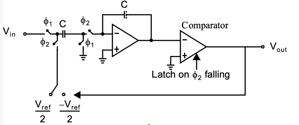
Sampling Filter. A sigma delta ADC is a type of sampling filter. This means we use z-domain discrete mathematics. The ADC has a signal transfer function (STF) and a noise transfer function (NTF). If we follow Figure 1 and label the input u(n) and the output y(n), then we have y(n)=(u(n)-y(n))*H(z)+e(n) which resolves to y(n)=u(n) This is equivalent to y(n)=u(n)*H(z)/(1+H(z))+e/(1+H). We choose to make H(z)=1/(z-1), an integrator, and then y(n)=z^-1*u(n)+e(1-z^-1). This means the input is delyed but the error is noise shaped by differentiator. A circuit implementation of the sigma delta is shown in Figure 2. It can be seen that a sigma delta can be realized with a minimum of cicuitry with nothing more than a sampling integrator and a comparator.
The use of switched capacitor circuits it prevalent in the development of switched capacitor circuits. The above detail was provided to provide a flavor for r the basis of AIStorm’s innovation.
Limitations of Switched Capacitor Circuits. The switched capacitor circuit in Figure 2 is a simplified representation of what is common to even more complex sigma delta converters. The circuits have two very specific failings: i) the circuit operates over two cycls which completely settle and ii) the amplifier limits the speed of operation. The switches are noise generators which integrate into an effective bandwidth of the R of the switch and C of the switched capacitor, every cycle. This provides a 2kT/C minimum voltage noise level. The amplifier also has a finite bandwidth and generates noise. As an example, if we were at 125C, and we wanted 16 bits of accuracy over a 1V dynamic range then our capacitor size would be C=2kT*2^16=2*1.38e-23*(273.15+125)*(2^16)^2=47pF. Additionally there is aliasing and other noise contributors so the result is a untenably large capacitors. The amplifier itself must offer a response every cycle causing a competition between its settling time and the amount of aliasing it contributes, generating additional noise. Additionally, the opamp and the capacitors waste a lot of power. Finally for higher order ADCs the matching requirement for capacitors is very difficult in production.
Charge Domain Advantage. Figure 3 shows AIStorm’s charge domain ADC. This ADC can be fit into a single pixel. The use of switch charge allows us to eliminate: i) the opamp; ii) the large capacitors and; iii).capacitor matching requirements. In fact not only do we gain the ability to use capacitors in the 10fF range instead of pF range (>100x smaller), but we also generate a -40db/dec sinc anti-blasing filter at no extra cost.
>50x Smaller. With the capacitor size reduces by >100x we can expect a 20x or greater size reduction. This allows sigma delta converters to enter applications they have not been able to enter in the past. For example in Figure 3 is a sigma delta converter designed by AIStorm which can fit into each pixel in an imager.
>20x Less Power. With less capacitance to fill, we transfer less charge through our voltage dynamic range. We also dont have opamps to power. The result is >20x less power than switched capacitor based sigma delta converters.
>10x Faster. Charge domain moves charge 2.5x to 10x faster than a transistor based solution. With less charge to move due to the smaller capacitors and this movement advantage, expects 10x or better speed improvements. For example multi-GHz ADCs where they were not possible before in a given process.
Conclusion. Charge domain dataconverters offer 100x smaller size, >20x less power, and can run >10x faster. Charge domain breaks the finite settling time limitations causing the excessive kT/C noise in switched capacitor implementations. AIStorm can help you build custom solutions to fit your applications or replace legacy solutions. Please contact your AIStorm sales representations today.